- 您现在的位置:买卖IC网 > Sheet目录1222 > ISL62386HIEVAL1Z (Intersil)EVAL BOARD FOR ISL62386HI 32TQFN
�� �
�
�ISL62386�
�maximum� input� voltage,� while� a� voltage� rating� of� 1.5x� is� a�
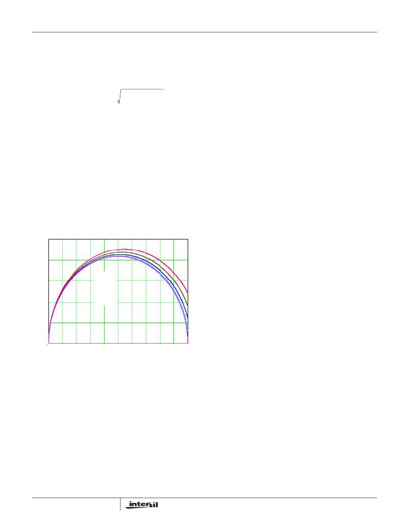
�preferred� rating.� Figure� 28� is� a� graph� of� the� input� capacitor�
�RMS� ripple� current,� normalized� relative� to� output� load� current,�
�as� a� function� of� duty� cycle� and� is� adjusted� for� converter�
�efficiency.� The� normalized� RMS� ripple� current� calculation� is�
�written� as� Equation� 22:�
�off,� the� high-side� MOSFET� turns� off� with� a� V� DS� of�
�approximately� V� IN� -� V� OUT� ,� plus� the� spike� across� it.� The�
�preferred� low-side� MOSFET� emphasizes� low� r� DS(ON)� when�
�fully� saturated� to� minimize� conduction� loss.� It� should� be�
�noted� that� this� is� an� optimal� configuration� of� MOSFET�
�selection� for� low� duty� cycle� applications� (D� <� 50%).� For�
�D� ?� k�
�I� C�
�IN�
�(� RMS� ,� NORMALIZED� )�
�2�
�12�
�I� MAX� ?� D� ?� (� 1� –� D� )� +� --------------�
�=� -----------------------------------------------------------------------�
�I� MAX�
�(EQ.� 22)�
�higher� output,� low� input� voltage� solutions,� a� more� balanced�
�MOSFET� selection� for� high-� and� low-side� devices� may� be�
�warranted.�
�P� CON_LS� ≈� I� LOAD� ?� r� DS� (� ON� )� _LS� ?� (� 1� –� D� )�
�Where:�
�-� I� MAX� is� the� maximum� continuous� I� LOAD� of� the� converter�
�-� k� is� a� multiplier� (0� to� 1)� corresponding� to� the� inductor�
�peak-to-peak� ripple� amplitude� expressed� as� a�
�percentage� of� I� MAX� (0%� to� 100%)�
�-� D� is� the� duty� cycle� that� is� adjusted� to� take� into� account�
�For� the� low-side� (LS)� MOSFET,� the� power� loss� can� be�
�assumed� to� be� conductive� only� and� is� written� as� Equation� 24:�
�2�
�(EQ.� 24)�
�For� the� high-side� (HS)� MOSFET,� the� conduction� loss� is�
�written� as� Equation� 25:�
�the� efficiency� of� the� converter� which� is� written� as:�
�Equation� 23.�
�P� CON_HS� =� I� LOAD�
�2�
�?�
�r� DS� (� ON� )� _HS� ?� D�
�(EQ.� 25)�
�V� OUT�
�D� =� --------------------------�
�P� SW_HS� =� -----------------------------------------------------------------� +� -------------------------------------------------------------�
�(EQ.� 23)�
�V� IN� ?� EFF�
�In� addition� to� the� bulk� capacitance,� some� low� ESL� ceramic�
�capacitance� is� recommended� to� decouple� between� the� drain�
�of� the� high-side� MOSFET� and� the� source� of� the� low-side�
�MOSFET.�
�For� the� high-side� MOSFET,� the� switching� loss� is� written� as�
�Equation� 26:�
�V� IN� ?� I� VALLEY� ?� t� ON� ?� f� SW� V� IN� ?� I� PEAK� ?� t� OFF� ?� f� SW�
�2� 2�
�(EQ.� 26)�
�0.60�
�Where:�
�0.48�
�-� I� VALLEY� is� the� difference� of� the� DC� component� of� the�
�inductor� current� minus� 1/2� of� the� inductor� ripple� current�
�0.36�
�0.24�
�0.12�
�k=1�
�k� =� 0.75�
�k� =� 0.5�
�k� =� 0.25�
�k=0�
�-� I� PEAK� is� the� sum� of� the� DC� component� of� the� inductor�
�current� plus� 1/2� of� the� inductor� ripple� current�
�-� t� ON� is� the� time� required� to� drive� the� device� into�
�saturation�
�-� t� OFF� is� the� time� required� to� drive� the� device� into� cut-off�
�Selecting� The� Bootstrap� Capacitor�
�The� selection� of� the� bootstrap� capacitor� is� written� as�
�Equation� 27:�
�Δ� V� BOOT�
�0�
�0�
�0.1�
�0.2�
�0.3�
�0.4� 0.5� 0.6�
�DUTY� CYCLE�
�0.7�
�0.8�
�0.9�
�1.0�
�Q� g�
�C� BOOT� =� ------------------------�
�(EQ.� 27)�
�FIGURE� 28.� NORMALIZED� RMS� INPUT� CURRENT� @� EFF� =� 1�
�MOSFET� Selection� and� Considerations�
�Typically,� a� MOSFET� cannot� tolerate� even� brief� excursions�
�beyond� their� maximum� drain� to� source� voltage� rating.� The�
�MOSFETs� used� in� the� power� stage� of� the� converter� should�
�have� a� maximum� V� DS� rating� that� exceeds� the� sum� of� the�
�upper� voltage� tolerance� of� the� input� power� source� and� the�
�voltage� spike� that� occurs� when� the� MOSFET� switches� off.�
�There� are� several� power� MOSFETs� readily� available� that� are�
�optimized� for� DC/DC� converter� applications.� The� preferred�
�high-side� MOSFET� emphasizes� low� gate� charge� so� that� the�
�device� spends� the� least� amount� of� time� dissipating� power� in�
�the� linear� region.� Unlike� the� low-side� MOSFET� which� has� the�
�drain-source� voltage� clamped� by� its� body� diode� during� turn�
�17�
�Where:�
�-� Q� g� is� the� total� gate� charge� required� to� turn� on� the�
�high-side� MOSFET�
�-� Δ� V� BOOT� ,� is� the� maximum� allowed� voltage� decay� across�
�the� boot� capacitor� each� time� the� high-side� MOSFET� is�
�switched� on�
�As� an� example,� suppose� the� high-side� MOSFET� has� a� total�
�gate� charge� Q� g� ,� of� 25nC� at� V� GS� =� 5V,� and� a� Δ� V� BOOT� of�
�200mV.� The� calculated� bootstrap� capacitance� is� 0.125μF;� for�
�a� comfortable� margin,� select� a� capacitor� that� is� double� the�
�calculated� capacitance.� In� this� example,� 0.22μF� will� suffice.�
�Use� an� X7R� or� X5R� ceramic� capacitor.�
�Layout� Considerations�
�As� a� general� rule,� power� should� be� on� the� bottom� layer� of�
�the� PCB� and� weak� analog� or� logic� signals� are� on� the� top�
�FN6831.0�
�February� 4,� 2009�
�发布紧急采购,3分钟左右您将得到回复。
相关PDF资料
ISL6291EVAL1
EVALUATION BOARD FOR ISL6291
ISL6292EVAL2
EVALUATION BOARD 2 ISL6292
ISL6296EVAL1
EVALUATION BOARD 1 ISL6296
ISL6298EVAL1
EVALUATION BOARD 1 ISL6298
ISL6298EVAL2
EVALUATION BOARD 2 ISL6298
ISL6299AEVAL1
EVALUATION BOARD 1 ISL6299A
ISL6411EVAL1
EVALUATION BOARD ISL6411
ISL6413EVAL1
EVALUATION BOARD ISL6413
相关代理商/技术参数
ISL62386HRTZ
功能描述:IC PWR SUPPLY CTRLR QUAD 32TQFN RoHS:是 类别:集成电路 (IC) >> PMIC - 电源控制器,监视器 系列:- 产品培训模块:Lead (SnPb) Finish for COTS
Obsolescence Mitigation Program 标准包装:2,500 系列:- 应用:多相控制器 输入电压:- 电源电压:9 V ~ 14 V 电流 - 电源:- 工作温度:-40°C ~ 85°C 安装类型:表面贴装 封装/外壳:40-WFQFN 裸露焊盘 供应商设备封装:40-TQFN-EP(5x5) 包装:带卷 (TR)
ISL62386HRTZ-T
功能描述:IC PWR SUPPLY CTRLR QUAD 32TQFN RoHS:是 类别:集成电路 (IC) >> PMIC - 电源控制器,监视器 系列:- 产品培训模块:Lead (SnPb) Finish for COTS
Obsolescence Mitigation Program 标准包装:2,500 系列:- 应用:多相控制器 输入电压:- 电源电压:9 V ~ 14 V 电流 - 电源:- 工作温度:-40°C ~ 85°C 安装类型:表面贴装 封装/外壳:40-WFQFN 裸露焊盘 供应商设备封装:40-TQFN-EP(5x5) 包装:带卷 (TR)
ISL62386LOEVAL1Z
功能描述:EVAL BOARD FOR ISL62386LO 32TQFN RoHS:是 类别:编程器,开发系统 >> 评估演示板和套件 系列:* 标准包装:1 系列:PCI Express® (PCIe) 主要目的:接口,收发器,PCI Express 嵌入式:- 已用 IC / 零件:DS80PCI800 主要属性:- 次要属性:- 已供物品:板
ISL62391
制造商:INTERSIL 制造商全称:Intersil Corporation 功能描述:High-Efficiency, Triple-Output System Power Supply Controller
ISL62391_11
制造商:INTERSIL 制造商全称:Intersil Corporation 功能描述:High-Efficiency, Triple-Output System Power Supply Controller
ISL62391CHRTZ
功能描述:IC PWR SUPPLY CTRLR 28TQFN RoHS:是 类别:集成电路 (IC) >> PMIC - 电源控制器,监视器 系列:- 产品培训模块:Lead (SnPb) Finish for COTS
Obsolescence Mitigation Program 标准包装:2,500 系列:- 应用:多相控制器 输入电压:- 电源电压:9 V ~ 14 V 电流 - 电源:- 工作温度:-40°C ~ 85°C 安装类型:表面贴装 封装/外壳:40-WFQFN 裸露焊盘 供应商设备封装:40-TQFN-EP(5x5) 包装:带卷 (TR)
ISL62391CHRTZ-T
功能描述:IC PWR SUPPLY CTRLR 28TQFN RoHS:是 类别:集成电路 (IC) >> PMIC - 电源控制器,监视器 系列:- 产品培训模块:Lead (SnPb) Finish for COTS
Obsolescence Mitigation Program 标准包装:2,500 系列:- 应用:多相控制器 输入电压:- 电源电压:9 V ~ 14 V 电流 - 电源:- 工作温度:-40°C ~ 85°C 安装类型:表面贴装 封装/外壳:40-WFQFN 裸露焊盘 供应商设备封装:40-TQFN-EP(5x5) 包装:带卷 (TR)
ISL62391CIRTZ
功能描述:IC PWR SUPPLY CTRLR 28TQFN RoHS:是 类别:集成电路 (IC) >> PMIC - 电源控制器,监视器 系列:* 产品培训模块:Lead (SnPb) Finish for COTS
Obsolescence Mitigation Program 标准包装:2,500 系列:- 应用:多相控制器 输入电压:- 电源电压:9 V ~ 14 V 电流 - 电源:- 工作温度:-40°C ~ 85°C 安装类型:表面贴装 封装/外壳:40-WFQFN 裸露焊盘 供应商设备封装:40-TQFN-EP(5x5) 包装:带卷 (TR)